Super-Resolution Infrared (IR) Imaging
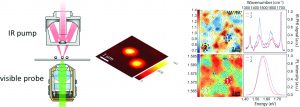
IR microscopy/spectrsocopy is an optimal tool for obtaining chemical-specific information of samples without the need for exogenous labels. However, conventional far-field imagining methodologies are diffraction limited in the IR with effective spatial resolutions of >5 μm. We have developed a novel far-field IR imaging technique based on photothermal heterodyne imaging (IR-PHI). In our approach, a pulsed IR pump laser excites the sample, resulting in a modulated photothermal change in the sample’s local environment. This change is probed by a counter-propagating visible/near infrared beam using lockin detection. Counter-propagating beam geometries allows for the use of high numerical aperture refractive visible objectives. This makes IR-PHI an IR imaging technique with spatial resolutions narrowed to the probe’s diffraction limit.
We have imaged and measured IR spectra of several soft matter systems (polystyrene beads, thin polymer films, and single Escherichia coli bacterial cells) with a spatial resolution of 0.3 μm, which is the highest spatial resolution reported to date for far-field IR imaging. We are now applying this technique to semiconductor systems including hybrid perovskite thin films and single layer graphene oxide and exploring the influence of compositional heterogeneity on the photophysics of these systems.

Single Nanostructure Extinction Spectroscopy
 Recent interest in the optical and electrical properties of nanostructures has led to the development of synthetic routes to these materials using ordinary wet chemistries. However, these methods lead to ensembles with significant inter-particle size distributions. These variations can lead to significant heterogeneity in the optical properties of these materials, especially in strong confinement regimes. While optical measurements of such ensembles have undoubtedly furthered the understanding of these nanostructures, the “averaged” optical response prevents a clear insight into their photophysics.
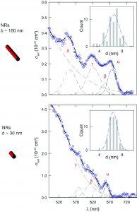
Single particle spectroscopy has therefore emerged as a powerful tool to circumvent problems associated with ensemble measurements. The most common among these are emission based approaches, offering the advantage of a being zero background experiments. They can therefore easily achieve single particle sensitivity. However, these techniques remain limited to fluorescent particles and are therefore not applicable to a large number of non-fluorescent materials. A large focus of our research therefore utilizes single particle absorption spectroscopy methods to probe and model single nanostructure electronic structure.
We use spatial modulation spectroscopy (SMS), a sensitive, low-noise approach that allows for the direct measurement of single nanostructure extinction spectra. The technique is based on the high frequency modulation of a particle’s position with respect to a diffraction limited laser’s focus. The small change in transmitted light intensity due to the sample’s movement in and out of the beam is measured using lockin detection at the modulation frequency. We utilize this technique to probe the absorption spectra of individual CdSe nanowires and nanorods, and model of their electronic structure.
Spatially-Resolved Photophysics of Hybrid Perovskites
Hybrid perovskites such as MAPbI3 (MA=CH3NH3+) and mixed halide perovskites such as MAPb(I1-xClx)3 and MAPb(I1-xBrx)3 represent a potential paradigm shift for creating low-cost solar cells. Intriguing aspects of these materials include large carrier mobilities, large power conversion efficiencies (PCEs), the ability to tune bandgap with halide composition, and the potential to manufacture these materials at low cost.
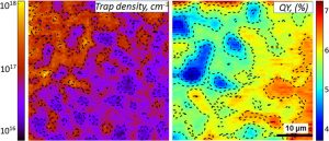
 Despite power conversion efficiencies that now exceed 22%, record PCEs are still far from their theoretical Shockley-Queisser limit of 31%. Hindering the realization of perovskite solar cells are a number of outstanding issues. The first is the lack of microscopic insight into solar cell performance beyond simple device-level metrics such as open circuit voltages (Voc), short circuit currents (isc), fill factors (FFs) and PCEs. The fact that hybrid perovskite solar cells are fully solution-processed means that spatial heterogeneities in device performance likely exist. Consequently, it is critical to understand local hybrid perovskite photophysics and their ultimate impact on device performance –for example, to see whether reported PCEs are representative of the cell or if instead they reflect the behavior of a small subregion of the active absorber layer. Doing so requires utilizing spatially-resolved analytical techniques that have heretofore been underdeveloped.
We are therefore conducting detailed spatially- and temporally-resolved absorption/emission microscopy measurements of hybrid perovskite thin films and devices. We see to elucidate and quantify limiting factors of hybrid perovskite solar cell performance that stem from local electronic disorder. This work includes efforts to address the origin of both anion and cation phase segregation in mixed anion and mixed cation hybrid perovskite films. It also includes work to understand the fate of photogenerated carriers in working devices. Finally, related work centers on understanding the origin of size-dependent Stokes shifts in the emission of hybrid perovskite nanocrystals.
Semiconductor Laser Cooling
Advances in refrigeration have been responsible for significant progress in science and technology. The discovery of Bose–Einstein condensation, superconductivity, superfluidity, and the fractional quantum Hall effect all result from the ability to reach low temperatures using gases of trapped ions and atoms. It is also essential to numerous modern technologies such as visible and infrared photodetectors, which require low temperatures for efficient operation. At present, minimum temperatures for Peltier-based solid state cryocoolers are limited to ∼170 K. Consequently, a pressing need exists to develop new solid state cooling technologies suitable for future optoelectronic applications.
The concept of condensed phase optical refrigeration has existed for nearly 90 years since Pringsheim first proposed cooling through phonon-assisted PL up-conversion. In semiconductors, this entails first creating a cold population of free electrons and holes using a laser tuned to the semiconductor band edge. Subsequent phonon coupling results in carrier excitation and leads to emission with energies greater than those of the incident laser. This removes thermal energy from the system and sets the basis for optical cooling. Despite the conceptual simplicity of the process, realizing optical refrigeration requires exacting parameters from the condensed phase medium. This includes near-unity external quantum efficiencies (EQEs) and corresponding up-conversion efficiencies, both aimed at suppressing unwanted background heating.
In this study, we are therefore investigating the potential laser cooling of CdS nanobelts as well as other high EQE nanostructures. The goal is to understand the origin of upconversion in these materials and to eventually demonstrate practical examples of condensed phase optical cooling.
Materials Development & Applications
Materials that we have focused on synthesizing include
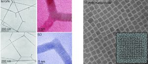
- Solution-based semiconductor nanowires. Representative systems include ZnSe, CdS, CdSe, CdTe, PbS and PbSe. The overarching challenge behind these studies has been to control crystallization at the molecular level in order to enable the direct bottom up growth of technologically relevant nanostructures.
- Two-dimensional semiconductor nanoplatelets. Motivating these studies have been the anisotropic physical, chemical and optical properties of 2D materials. Although two-dimensional carbon is the best known 2D system, there is now an active search in the field to find unique materials beyond graphene. Representative systems we have made include Cu2-xSe, Cu2SnS3, TiS2 and corresponding molybdenum carbamate compounds.
- Colloidal quantum dots. Representative materials include CdSe and CsPbBr3.

